Monday, May 18, 2009

Intel DX58SO X58 Express Chipset Motherboard Review

Introduction To The DX58SO


Image Description

Intel chipset-based motherboards have always been some of the most reliable boards on the market. Not only that, but Intel chipset-based motherboards that are produced by Intel have always been some of the most feature rich and durable boards on the market. Intel could easily sit back for a bit and rest on their laurels, but they don't; they keep pushing ahead with constant innovation. That innovation has brought them to their newest chipset, the Intel X58 Express chipset, and the Intel DX58SO Motherboard.

The Intel DX58SO chipset, coupled with the ICH10R southbridge, brings the best and greatest that Intel has to offer to a quality designed motherboard that will bring the end user all the performance, speed and capabilities to make their computing experience all that it can be.

Let's take a look at the specs...

Specs

Form factor ATX (12.00 inches by 9.60 inches [304.80 millimeters by 243.84 millimeters])
Processor Click View supported processors for the most current list of compatible processors.
At product launch, this desktop board supports:
Memory
  • Four 240-pin DDR3 SDRAM Dual Inline Memory Module (DIMM) sockets
  • Support for DDR3 1600 MHz, DDR3 1333 MHzς, DDR3 1066 MHz
  • Support for up to 16 GB of system memory
Chipset
Audio Intel® High Definition Audio subsystem in the following configuration:
  • 10-channel (7.1) Dolby Home Theater* Audio subsystem with five analog audio outputs and two S/PDIF digital audio outputs (coaxial and optical) using the Realtek* ALC889 audio codec
Video
  • Nvidia SLI* and ATI CrossFire* multi-GPU platform support enables two graphics cards to work together for ultimate 3D gaming performance and visual quality
  • Full support of next-generation ATI CrossFire* and Nvidia SLI*
LAN support Gigabit (10/100/1000 Mbits/sec) LAN subsystem
Peripheral interfaces
  • Twelve USB 2.0 ports (8 external ports, 2 internal headers)
  • Six Serial ATA 3.0 GB/s ports, including 2 eSATA port with RAID support supplied by a Marvell* controller
  • Two IEEE-1394a ports (1 external port, 1 internal header)
  • Consumer IR receiver and emitter (via internal headers)
Expansion capabilities
  • One PCI Conventional* bus add-in card connectors (SMBus routed to PCI Conventional bus add-in card connector)
  • One primary PCI Express* 2.0 x16 (electrical x16) bus add-in card connector
  • One secondary PCI Express 2.0 x16 (electrical x16) bus add-in card connector
  • One PCI Express* 1.0a x16 (electrical x4) bus add-in card connector

Intel also supports this board with a three year limited warranty.

Saturday, April 18, 2009

Intel's 925XE Chipset & 1066FSB Processors Arrive

Finally... 1066FSB Arrives

The move from the Intel 865/875 chipsets to the more recent 915/925 chipsets brought noted improvements across the board that no one could ignore. Today (Halloween by chance) is the day that Intel makes public the updated 925X chipset and the new processor that can capitalize on it. Enter the 925XE Express Chipset and Pentium 4 Processor Extreme Edition with HT Technology at 3. 46GHz (13x266MHz). For those of you who don't know the Intel Pentium 4 processor has been running at a Front Side Bus (FSB) of 800MHz for some time now. To achieve this speed Intel was running the FSB quad pumped at 200MHz. Since the FSB dictates how much data can travel between the CPU and chipset, an increase is logical to gain overall system performance. Today Intel raises the bar on FSB performance and for the first time breaks the 1GHz barrier by running the FSB quad pumped at 266MHz, thus arriving at a FSB of 1066MHz.

The increase to a 1066MHz FSB will be the first time DDR2 memory will officially run in sync at DDR2 533MHz. Plus, now that DDR2 memory has matured seeing 3-3-3-8 timings with PC2-4200 memory is common. It is no shocker that Enthusiasts have been waiting months for this chipset, but we found it interesting that many companies have also been waiting on the 925XE chipset. The most noticeable is ABIT, who is going to launch the first ABIT-Fatal1ty gamer motherboard based on the 925XE chipset, thus gambling the success of their new product line off this chipset. The long-awaited FSB speed increase has arrived! Was it worth the wait?

If you look at what Intel has said about their Socket 775 it is their long term solution platform. They have made public comments at the Intel Developer Forum and other events that the 915/925 chipset family will more than likely power Intel's next generation dual core processors. These new processors are expected to come out in mid 2005 -- best guess would be late Q2 or early Q3. Between now and then the Intel 925XE looks to be the Intel enthusiasts' chipset of choice for their next system build.

The New Intel 3.46GHz EE 1066FSB Processor:

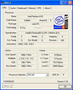
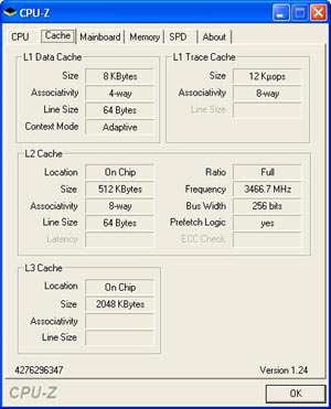
The new Intel 3.46EE processor is based on the old 130nm Northwood core (also known as P4 "C"). It comes with 2mb of L3 Cache and does not have SSE3 or XD-BIT instructions. The 3.46GHz processor only differs from the previous generation Extreme Editions by being able to run at 266MHz on the FSB. We actually tried to run our "old" 3.4EE at 13x266MHz and it failed to successfully load Windows at such speeds. The new Intel 3.46EE is basically a cream of the crop Extreme Edition processor that can run at a high front side bus frequency.

Let's take a look at pricing for 1,000-Unit quantities and also compare the new 3.46GHz EE to some other socket 775 prices.

  • Pentium 4 3.46EE 1066FSB - 3.46GHz -- $999
  • Pentium 4 3.40EE 800FSB - 3.40GHz -- $925
  • Pentium 4 560 - 3.60GHz -- $417
  • Pentium 4 550 - 3.40GHz -- $278

As you can tell the new Pentium 4 3.46EE is not close to the price range for any college student (wouldn't it be nice if Intel offered student discounts like Microsoft??), but is priced just like the original P4 3.4EE when it came out several months ago at $999. That happens to be more than double the Intel 560 processor, which is the flagship of the "mainstream" Intel socket 775 processors.

Below are some shots of our Intel 3.46GHz EE processor running on our test bed.


Intel 3.46EE CPU Specs


Intel 3.46EE Cache

While the Pentium 4 Extreme Edition will be the first and currently only processor to work with the new quad-pumped system bus at 266 MHz there are more processors coming. Intel also affirmed that its Pentium 4 Extreme Edition (EE) 3.73GHz and 600-series desktop CPUs, which should be launched in the first quarter of next year, will feature Intel's Extended Memory 64 Technology, or Intel EM64T. We asked about XD-BIT (Execute Disable bit) and were told not to expect any of the current P4 EE's to come with it, just the Prescott processors with a 'J'-suffix will have XD-Bit enabled. All the enthusiasts looking for a "mainstream" cost efficient 1066FSB processor will have to wait till the 600 series is launched!

Let's move on and see what the new Intel reference board offers.

Intel 6xx Series Processors Arrive

Intel 6xx Series CPU's Arrive With New Features!

Intel Pentium 4 660 Processor

Over the holiday weekend Intel officially announced the new Pentium 4 Extreme Edition 3.73GHz processor and four processors in their Pentium 4 6XX series (rated as 660 to 630). Today we have the Intel Pentium 4 Extreme Edition at 3.73GHz and the Intel Pentium 4 660 in house for testing. Both of these processors use a new Prescott core that features 2MB of L2 cache and are EMT64 enabled!

When the Prescott first came out the longer pipelines and the increased temperatures from the new 90nm core shocked even the most die hard Intel fans. With the Intel P4 6XX series Intel strived to add performance while at the same time lowering power consumption and temperatures. The new improved core is still manufactured using the 90nm strained silicon production technology just like the original Prescott, which has been in use on the Pentium 4 5XX processors for almost a year now. Since the Prescott core is by no means new or unknown let's jump right into the new features.

The New Features:

  • More L2 Cache - Enthusiasts know that more cache means more performance and that is exactly what Intel did on these updated Prescott cores. They doubled the L2 cache in hopes of adding performance. The extra cache means more transistors, and in this case, over 40 million more! This increase in cache also increases the size of the die from 112mm2 to 135mm2. This is the only true "performance" upgrade made to the core this time around.
  • EMT64 Enabled - Other than the extra L2 cache the newly launched Pentium 4 6XX processor family offers support for Enhanced Memory 64 Technology or EM64T as many know it by. Since this is nothing more than 64-bit extensions of x86 architecture they are identical to the AMD64 extensions, thus giving us the first AMD vs. Intel battle on the 64-bit Operating System. Now that both Intel and AMD have their 64-bit CPU's out the door and both are fully functional, with the latest public release of Windows XP Professional x64 expect to see this OS completed in the near future!
  • Enhanced Power Management - Combination of EIST (Enhanced Intel Speedstep Technology), C1E (Enhanced Halt State), and TM2 (Thermal Monitor 2). In an appropriately designed system, these features can deliver average power savings with little impact to performance by adjusting frequency & voltage. To go a little more in depth, all three technologies offer similar functionality initiated in three different ways. C1E is activated via Halt (idle) instruction execution. EIST operates via OS request based upon CPU load. TM2 operates via processor request based upon the thermal load on the processor.
  • Execute Diable Bit Enabled - Intel Execute Disable Bit offers Improved Security when used with Windows XP SP2. With the Execute Disable Bit feature you can be protected from certain types of viruses and buffer overflow exploits. This is similar to AMD's NX technology and Intel has used Execute Disable Bit on the 5XXJ series processors.

The die increase that we talked about above can be seen below via the images of the old Prescott core and the Prescott 2MB with extra cache:


Prescott w/ 1MB L2


Prescott w/ 2MB L2 Cache

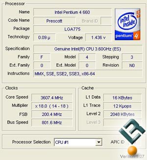
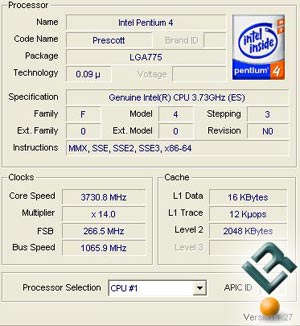
As you can see the new core is very similar to the old core. From just looking at the die pictures it seems as if they just added more cache and made some other minor changes. Below are CPU-Z version 1.27 screen shots of our two processors that we are showing you today.


Intel Pentium 4 660


Intel Pentium 4 3.73GHz EE

Both of our processors have 2048 KBytes of L2 Cache and are based on 90nm core technology. Both CPU's also feature a stepping code of 3 and a revision number of N0. The biggest difference between these two processors is the Bus Speed that they run at. The 660 is running at 800MHz, while the 3.73GHz EE is at 1066MHz. One more difference that can't be seen here, but can easily be spotted when you try to pay for these is the price difference. The Intel 3.73GHz Extreme Edition is priced at $999 in 1,000 unit quantities while the Intel 660 rings in at $605.

Many of our readers are enthusiasts that love overclocking so I know what you are thinking by this point -- An extra $400 for 66MHz FSB? I'm sure every overclocker out there just got a big smile on their face and so did we when we noted that the Intel Pentium 4 630 runs at 15 x 200 = 3.0GHz and costs only $224! With a multiplier of 15 and a sub $250 price this processor may easily hit close to a 1066MHz Bus Speed for less than a quarter of the price of the 3.73GHz Extreme Edition. As always you have to have the right hardware to overclock and don't forget it may void your warranty, increase temperatures, and overclocking is not endorsed by Intel. (Who themselves allow for overclocking up to 10% in their own boards BIOS options.)

Intel Dual Core: Multi-Tasking Benchmarking

Real Life Testing

Intel Pentium D Extreme Edition 840
The Pentium Extreme Editon


The New Champ On Top: Intel Pentium EE 840

Last week when the dual core embargo was lifted LR brought you the usual processor article on the Intel 840. Today, we are going to focus on the multi-tasking abilities of the new dual core Smithfield processor versus that of the single core Prescott. For benchmarking we wanted identical clock speeds, so an Intel 840 was run versus an Intel 640. Both processors are very similar having EIST, EMT64, 2MB Cache, 800MHz FSB's, and 90nm cores. The only major things that these two processors don't have in common are price points ($285ish on the 640 and around $1000 for the 840) and the fact that one is dual core. The following benchmarks should show the advantages of dual core over single core if one is to be seen.

Over the past week we have had hundreds of e-mails on what to test for multi-tasking and to be honest 99% revolved around gaming and virus scanning. The other e-mails dealt with watching DVD's, downloading files from the internet, running Folding @ Home, Encoding DVD's, and other multi-tasking situations.

Software Used:

  • Microsoft Media Player 10
  • Power DVD 6
  • DVD Shrink 3.2.0.15
  • EZ CD Ripper 2.30
  • Folding @ Home Console 5.02
  • Symantec Norton 2004
  • DOOM 3

Test System:

  • Intel P4 640 & 840 -- Intel D955XBK (Intel 955X), 1GB (2x512MB) Corsair PC5400 @ DDR2 667 (3-2-2-8), Geforce 6800GT 256mb (Forceware 71.84), 120GB Seagate SATA150 HDD, Windows XP w/SP2 and DX9C.

Testing Procedure:

All testing was done on a fresh install of Windows XP Professional build 2600 with Service Pack 2 and DirectX 9.0c. All benchmarks were completed on the desktop with multiple applications open. No overclocking was done on the video card during any of this review.

Time to see how dual core works in a multi-tasking environment.

The Intel Pentium D 820..... Dual Core for the masses

Introduction

The Intel Pentium D 820

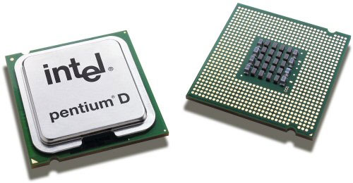
Two months ago, after almost a year of hype, dual core processors made their general public debut. With the release of Intel's Pentium D 840, those who could afford the best of the best finally saw the benefits that dual core processors bring to the table. Today, with Intel's release of the Pentium D 820, Intel brings the benefits of dual core processors to the rest of us. What benefits can you expect from Intel's newest, much hyped processor? Is upgrading from a 5XX or 6XX series processor worth it right now?

Today, Legit Reviews will answer these questions, and give you our impression of Intel's budget dual core processor, the Intel Pentium D 820. Featuring a 2.8GHz core speed and 1 MB of L2 cache, the 820 not only promises vast improvement over hyper-threading when multitasking, but also a "smoother" performance in single thread applications

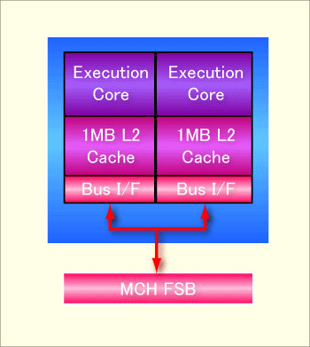
Pentium D core layout

A few notable features, or lack of features, are the absence of hyper threading and the lack of EIST (Which makes sense as the Pentium D 820 is already throttled back to 2.8 GHz). Will the lack of Hyper Threading show much difference in overall performance? We'll see later on as we test the Pentium D 820 against its bigger brother the Pentium D 840, as well as the Pentium 4 620.

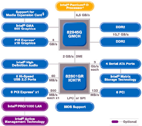
The intel 945 G chipset

With the release of the Pentium D 840, users realized a major drawback to dual core processors, the lack of support with the 915 and 925 chipsets, so those of us who shelled out upwards of $200 a few months ago for a high end 925XE board are basically SOL. As of right now, only the 945 and 955 chipsets will support dual core processors. Which brings me to the next portion of this review.....the 945 chipset. As it did with the Pentium D 840 and 955 chipset, Intel released the Pentium D 820 with its optimized partner, the 945 chipset. Like the 865 and 915 chipsets before it, the 945 is a watered down version of Intel's current flagship chipset. Released in two versions, the "G", which has integrated graphics, and the "P", which does not, the 945 chipset incorporates almost all of the features found on its expensive big brother, the main exception being Intel's patented Memory Pipeline Technology (As Intel states, "Enhanced memory pipelining that enables a higher utilization of each memory channel, accelerating data transfers between the processor and system memory and resulting in higher system performance.").

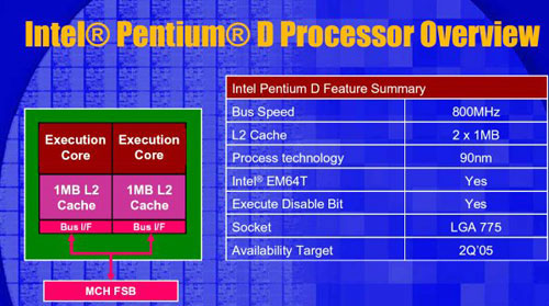
Pentium D overview

Part 1: Intel Pentium Processor Extreme Edition 955

Intel Unleashes the Presler Processor

Usually around this time of the year we show you dozens of benchmarks with the next generation Intel Processor with the whole AMD versus Intel mentality. Legit Reviews is still going to do that, but just not today. This morning at 10am Intel announced its new Pentium Processor 955 Extreme Edition CPU, formerly code-named Presler. This chip, which goes on sale to the public on January 16 for $999, is the second generation of dual-core consumer desktop CPU's from the chip giant. Intel has made a number of changes to it's dual core processor series and many will call this Intel's first true dual core processor. This processor features two separate cores with 2MB L2 cache each for a total of 4MB, a 266MHz Quad Pumped Front Side Bus for a solid 1066MHz system bus, Intel Virtualization Technology, and it was all done on the 65nm process over the previous 90nm package found on the previous Prescott and Extreme Edition processors.

The Intel Pentium Extreme Edition 955 Processor

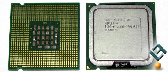
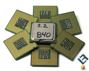
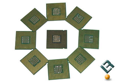
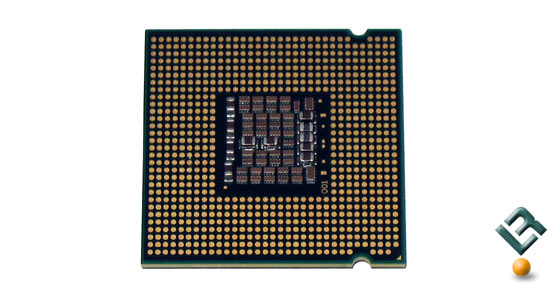
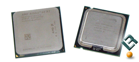
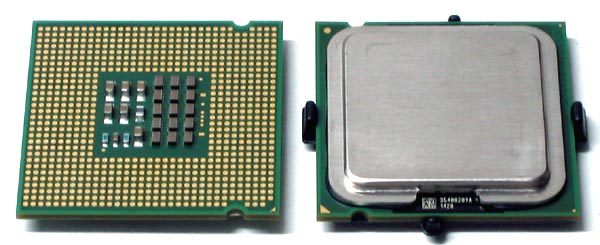
After getting the Intel Pentium Processor 955 Extreme Edition "Presler", holy cow that is a mouthful, we quickly found out that a couple rumors going around the internet were not true. One was about the temperatures and the other being the overclockability of the processor in general. Without further ado let's look at the new gem in Intel's Enthusiast portfolio. Taking a look at the Presler (Shown above in the middle) we can easily notice that it looks different from the Intel 5xx, 6xx, and 8xx processors that surround the new kid on the block. Let's see if CPU-Z can read the processor correctly.

A CPU-Z Shot of the Intel 955 Processor

It looks like CPU-Z is showing everything okay except for the voltage that the Vcore is running at. Our unlocked processor is running at a multiplier of 13 with a front side bus (FSB) of 266MHz for a total core frequency of 3.46GHz. Not a bad core speed for a CPU having doubled the cache than the previous Extreme Edition, which was the Intel 840 with a total cache of 2MB.

Intel Pentium Processor 965 Extreme Edition Review

The Extreme Edition Gets A Speed Bump

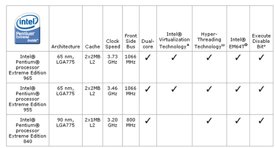
Like its predecessor, the Intel Pentium Processor Extreme Edition 965 with Hyper-Threading technology boasts 1066 FSB, 4 MB total L2 cache configured as 2 x 2MB per core, Intel Virtualization Technology, Execute Disable Bit, and Intel Extended Memory 64 Technology. The Extreme Edition platform provides the horsepower and new capabilities that allow PC enthusiasts the flexibility to address the robust content creation and multitasking expectations of the high-end desktop market segment. Below is a chart comparing the latest Extreme Edition processor to the previous two flagship processors that it has replaced.

The Intel 965 Processor

According to the above chart the only difference is the clock speed, but Intel has changed more than just the final frequency on the Extreme Edition.

Intel Pentium Processor Extreme Edition 965

  • 3.73 GHz dual core processor with Hyper-Threading Technology
  • 1066 FSB
  • 4 MB total L2 cache configured as 2 x 2MB per core
  • Intel Virtualization Technology
  • Execute Disable Bit
  • Intel Extended Memory 64 Technology (EM64T)

The Intel 965 Processor

The 965 comes clocked at 3.73GHz (14.0 x 267MHz) with a 1066MHz front side bus. If this clock frequency rings a bell it should as it is the same core speed as Intel's fastest single core Extreme Edition processor, the Prescott-based chip Intel 3.73GHz EE that was launched in Feburary 2005. There are two separate 'Cedar Mill' cores on the same package that make up the Presler core. Many call the Presler the first true dual-core Intel processor.

If you are thinking of getting one of these processors Intel recommends using the Delta EPS12V 600W ? DPS-600MB M power supply or equivalent with a 2x4 (instead of a 2x2) 12V2 connector to provide headroom and allow for more current and power to be delivered to the processor. The processor Vcc, Icc, and power specifications provided with the Intel Pentium Processor Extreme Edition 955 still apply to the new Intel Pentium Processor Extreme Edition 965. Now that we know what the Intel 965 is all about let's take a look at the new stepping.

Overclocking The Intel Pentium D Processor 805

Intel's Entry Level Dual-Core Processor: Pentium D 805

Image Description

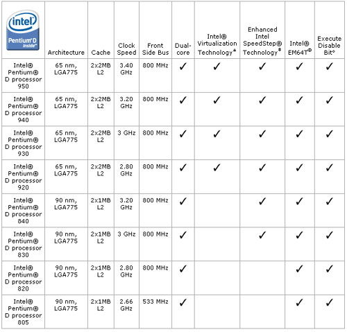
On April 7th, 2006, Intel silently launched the Intel Pentium D 805 processor. That makes the Pentium D 805 processor the entry level dual-core CPU for any Intel platform. Running at 2.66GHz the Pentium D 805 utilizes a Front Side Bus (FSB) of 533MHz and a clock multiplier of 20. To make this an entry level processor Intel gave it a 533MHz FSB, which is a slower than the other dual-core processors that all run on a 800MHz FSB and it does not have Enhanced Intel SpeedStep technology for better thermal regulation.

What does this mean to you? It means that Intel has released a dual-core processor priced at under $130. We couldn't ignore this budget dual-core processor and ordered one from chiefvalue.com this past week and it has been on the test bench since it arrived!

Image Description

The Intel Pentium D Processor 805 runs at 2.66GHz with a 533MHz FSB and shares two seperate 1MB L2 caches that are located on the procesor. The 805 is a Smithfield dual-core processor and does fully support 64-bit computing via the Intel EM64T technology.

Image Description

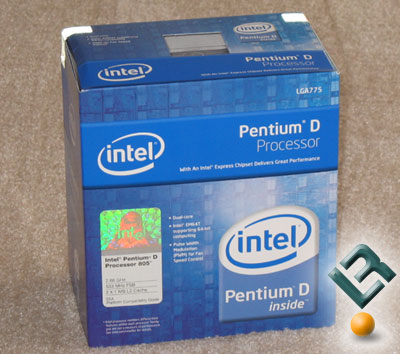
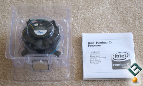
Inside the retail packaging you get the processor, an Intel heat sink fan cooling unit, and the owners manual with the Pentium D sticker on the back. Now that you know what you get for ~$130 US let's take a closer look at our processor and start the overclocking.

Intel's Common Building Blocks For Notebooks

Intel's Common Building Blocks

Image Description

At the start of 2006 Intel launched their Common Building Blocks (CBB) program for whitebook computers and today Legit Reviews takes a look at how far Intel has come after the program has been around for nearly six months. The CBB program promotes the use of industry-accepted mechanical and electrical specifications a number of critical notebook components, or ?ingredients". What does this mean for consumers and system builders? It means that notebooks will have interchangeability much like we have in desktop computers today. While the idea is far from new Intel has been the one to step up to the plate and do something about it.

The Intel CBB program consists of:

  • A Web site to provide a centralized repository of information about the program, participants, and platform and ingredient specifications
  • A continually updated list of CBB-compliant ingredients (submitted by suppliers)
  • A testing and verification service for candidate products
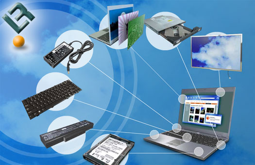
Image Description

Intel?s chief objective for the CBB program is to help expand the availability of a common set of cost-effective notebook computer ingredients, to reduce the risk of platform integration, and to stimulate the overall growth of the notebook market segment. The CBB has successfully developed a set of standards for the components that whitebooks use. Intel currently has set guidelines for the hard disk drive (HDD), optical disk drive, liquid crystal display (LCD) panel, battery pack, AC/DC adapter, keyboard, and requires a customizable notebook panel. Standardizing such components has been something many systems builders, who are looking at ways to reduce inventory and better service their customers have been wanting to do for years.

Image Description

Intel has a verification program in place that looks at notebooks built to be in the CBB program and our sources inside Intel let us know that it works and has caught a number notebooks trying to get around the system. Here is the list of barebone notebooks that have been tested for the interchangeability of the seven Common Building Block (CBB) components and have passed testing on all seven areas.

  • Asus S62Fp
  • Asus S62J
  • Asus S96F
  • Asus S96J (Pictures and Pricing)
  • Compal HGL 30
  • Compal HGL 31
  • Compal HEL 80
  • Compal HEL 81
  • Quanta SW1 (Pictures and Pricing)
  • Quanta TW3A
  • Quanta TW3M

Intel also has tested the following whitebook notebooks and found that they offer interchangeability of four Common Building Block (CBB) components. The following six notebooks have not passed testing for the AC/DC adapter, keyboard, and customizable notebook panel.

  • Clevo M660N
  • Clevo M665N
  • Gigabyte W451U
  • Gigabyte W551A
  • Gigabyte W551U
  • MSI 1034

In closing I have just got my hands on the ASUS S62J notebook, which has passed the verification process and is in the CBB program. When trying to order the customizable notebook panels from FedEx Kinkos I was unable to get my order placed after picking out my panel choice and entered all of my credit card information. The panels are all $15.10 at FedEx Kinkos and even allow for custom art work to be uploaded. The panels are treated with a pressure-sensitive adhesive on the back side for permanent or replaceable attachment, depending on the desired result. I'd like to use the replaceable adhesive, but FedEx Kinkos only carries permanent panels.

Other than the ordering issues with the panel the program seems to be working out nicely for Intel other than the fact that no one knows about it. Since profit margins have become so thin on notebooks and the fact that they tend to require more support than desktops many system builders haven't jumped on the notebook bandwagon. If you are one of those builders you might want to take a closer look at the 11 notebook models that are in the CBB program. With interchangeable parts it means you can stock one keyboard or battery and it will work on all of the notebooks! The Intel CBB program makes whitebook notebooks easy to service and support.

Other than customization and easier service Intel has also said these 11 notebooks are upgradeable. At first one might think that Intel means these notebooks can have more memory or a faster processor installed, but that is not the case here. Each of the 11 notebooks will support Intel's next generation dual-core mobile processor. Right now they all run Intel's Core Duo (Yonah) processors, but after a simple BIOS flash they will be able to support Core 2 Duo mobile processors (Merom). Speaking of Merom, how does a 20% performance improvement in 3DMark05 over the current Yonah processors sound? If you are looking for a notebook that wont be out dated, customizable, and easy to find parts for you have found your short list of whitebox computers.

in our forums. For those who are interested in building a whitebox notebook we have a thread listing all of the ones we can find in If you are curious about what companies make whitebox notebooks please check out this threadthis thread. As always feel free to post up any comments in our forums!

Intel Unleashes Conroe: X6800 and E6700 Reviewed

Let Me Introduce The New King Of The Hill: Conroe

Let me start off my saying that AMD has been the processor to have for gamers and enthusiasts over the past couple of years without a doubt. When Intel launched the Prescott core you could literally feel the breeze caused by consumers going from the Intel fan boy camp to the AMD side. The Intel Prescott faimly of processors were leaky and I even published an article examining prescott temperatures nearly three years ago explaining why the core temperatures were high. From the time the original Prescott core was launched till the end of it?s life the updates that Intel made to the core were nothing less than amazing. The initial Prescott processor that I reviewed back in 2004 was nothing like their last major update of the Prescott core one year to the month later in 2005. By adding more L2 cache, support for Enhanced Memory 64 Technology (EM64T), Execute Disable Bit, and the combination of EIST (Enhanced Intel Speedstep Technology), C1E (Enhanced Halt State), and TM2 (Thermal Monitor 2) the updated Prescott was finally looking like a production processor from Intel. The only problem was the fact that a year went by and since enthusiasts upgrade more than once yearly this was not a good move for Intel. While Intel was busy updating their desktop processor lines, AMD was busy playing catch up and consumers were jumping ship.

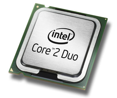
Intel Core 2 Duo Processor

Early this decade Intel had the performance lead and Intel processors came at a price premium as a result. Thanks to this AMD was kept alive early on by pricing their mainstream Athlon XP processors at near $100 and their market consisted mainly of dedicated enthusiasts and gamers looking for performance on a budget. I was one of those consumers back in the day and found that the first Athlon XP processors allowed great overclocking by having unlocked multipliers (RIP my beloved Athlon XP AGOIA stepping 1600+). Those are the days when VIA KT333 chipsets were the chipset to have and having 80mm delta screamers were the "in" thing. When AMD moved over to the Athlon 64 series they placed the memory controller on the processor itself and their new core turned out to be faster than Intel?s processors in a number of benchmarking scenarios, especially when it came to gaming performance. AMD saw what their main consumer group was doing with their processors and answered with a knock out blow at a time when Intel was promoting a leaky processor that came at a higher price. AMD Athlon 64 processors was crowned the CPU to have when it came to gaming computers and consumers were willing to pay whatever the price to have one.

The next race for both processor companies was marathon race to have dual-core processors. Intel won the race by bolting two Prescott processors together, which to this day leaves us wondering if it was worth it, but that is water under the bridge now. AMD came out with their dual-core processors dubed X2's a little later and once again had the performance to roll over Intel?s dual-core processors. AMD was able to take over the market lead for processor sales and the days of cheap AMD processors with unlocked multipliers across the board were long gone. AMD was now the lean mean fighting machine in green and was starting to give Intel a taste of what it feels like to be second in the processor market.

When you spent time at the top and have tasted victory it leaves a bitter sweet taste in your mouth. It's that sweet taste left in your mouth that you want back and the folks at Intel have just started to get their spot on top of the mountain back. Just this week Intel took the crown from AMD for being the number one processor in U.S. retail market for June and that's with the current processor lineup!

Today, Intel is introducing their next generation processor codenamed Conroe. This processor has had the most hype that I have ever seen and honeslty I jump right out and say that it doesn't fail to impress. Sit back and grab a pint or a tea and examine what just might be the next processor in your computer system.

$300 Gaming CPU's: AMD 5000+ Versus Intel E6600

I have $300 to spend. E6600 Conroe or 5000+ AM2?

Last week Intel introduced their Core 2 Duo Processors and Legit Reviews covered the announcement by releasing our thoughts on the Intel Core 2 Extreme Processor X6800 and the Intel Core 2 Duo Processor E6700. Both of the processors are at the top end of performance for desktop computers and come with top pricing as the X6800 running $999 and the E6700 coming in at $530. In case you missed our article here is a chart of Intel's upcoming processors and their pricing.

Processor
GHz
FSB
Cache
Package
July 23rd Price
X6800 2.93GHz 1066MHz 4M LGA775 $999
E6700 2.67GHz 1066MHz 4M LGA775 $530
E6600 2.4GHz 1066MHz 4M LGA775 $316
E6400 2.13GHz 1066MHz 2M LGA775 $224

With AMD being very open about their upcoming price cuts I figured that now would be a great time to look at the rumored prices that are all over the internet this week.

Processor
GHz
HT
Cache
Package
July 24th Price
FX-62 2.8GHz 2000MHz 2 x 1MB AM2 $799
5000+ 2.6GHz 2000MHz 2 x 512KB AM2 $299
4600+ 2.4GHz 2000MHz 2 x 512KB AM2 $224

According to rumors and leaked information on the internet we are able to see that AMD is going to be cutting prices next week and the price cuts are serious. AMD does not want to give up the price versus performance segment and if these prices turn out to be true we know AMD is serious! Most of today's gamers play on a budget and are finding themselves with their graphics card as the most expensive piece of hardware in their gaming system. Today we take a look at a processor that gamers can actually afford those that are in the $300 price range. That means the E6600 from Intel and the 5000+ by AMD have to fight to the death to see who's the stronger gaming processor. Below the AMD Athlon 64 X2 5000+ AM2 and the Intel Core 2 Duo Processor E6600 meet for the first time and size each other up.
Intel E6600 and AMD 5000+ AM2

The Intel Core 2 Duo processor E6600 still features the larger 4MB cache size and comes priced just over $300 at $319. To compete with the Intel Core 2 Duo processor E6600 AMD is going to price down their AMD Athlon 64 X2 5000+ AM2 processor to just under $300. It's also interesting to note that the 5000+ is running at 2.6GHz, which is 200MHz faster than the clock speed on the 2.4GHz E6600 processor from Intel. It's been a long time since I've run gaming benchmarks where the AMD processor has a faster clock speed. It should also be noted that the AMD processor has 1MB of cache where the E6600 has 4MB.

Without going crazy on the technical details let's take a look at our test system and then see what processor deserves to be in our gaming PC. Since gamers use real resolutions like 1280x1024 and 1600x1200 with AA and AF enabled we ran our benchmarks with settings that you would use at home.

Let's take a look at our test systems and then jump into the games!
Overclocking the Intel Core 2 Duo E6300 Processor

For $193 a Allendale Can Be Yours!

With the Intel Core 2 Duo E6300 priced under $200 it's the processor that many mainstream and budget shopers are picking up for use in their back to school computer systems. We have found that this entry level Intel Core 2 processor might cost just $193 , but the performance that it offers is much more than what you're paying for. With a little extra work and buying the right motherboard the Intel Core 2 Duo E6300 is by far one of the best overclocking processors that we have ever seen on the test bench here at Legit Reviews. Today Legit Reviews takes the Intel Core 2 Duo E6300 Processor and overclocks it to see what that means in terms of real world performance.

Image Description

When it comes to pricing the Intel Core 2 Duo Processor E6300 is still selling for a slight premium on the market, but rightfully so as you will soon find out. According to the July 27th,2006 price sheet the E6300 processor lists for $183 when purchased by the thousand, so the market price of $193 isn't that much of a premium for buying a single processor. With the E6300 retailing for under $200 it's attainable by many, but with the Core 2 Duo Processor family does come some issues.

One of the main stumbling blocks for Conroe and Allendale is the lack of chipset options and the few number of boards on the market. If you want run NVIDIA SLI graphics and an Intel Conroe/Allendale based processor you are limited to one board choice that is currently available on the market and that is the ASUS P5N32-SLI SE Deluxe motherboard. All of the other boards use the Intel 975x or 965x chipsets, which both support ATI's CrossFire technology. For our overclocking adventures we stuck with the Intel D975XBX 'bad axe' reference motherboard as it's known for it's overclocking abilities within reason and is readily available. We did have to do some minor adjustments to our motherboard to help out overclocking functionality, but our modifications can be done by anyone that can use a pen or pencil.

Intel Core 2 Duo Processor T7600 on the Dell XPS M1710

Running the Intel T7600 on the Dell XPS M1710

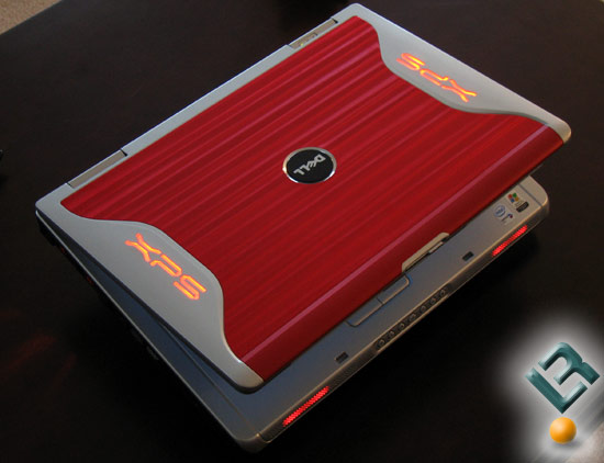
Laptops around the world are getting a performance boost as systems based on Intel Centrino Duo mobile technology are now shipping with Intel Core 2 Duo mobile processors starting today. With the launch of a new core many would suspect that a new socket or some sort of platform change would be needed, but that is not the case with the Core 2 Duo family of mobile processors. All that is needed is a BIOS update for the motherboard in the current Duo notebooks and all should be well. In all honesty I was able to install an Intel Core 2 Duo processor in our Do-It-Yourself based Clevo M570U 17" gaming notebook (Read the Review) and on our personal Dell XPS M1710 Special Edition Formula Red gaming notebook with no BIOS updates at all.

The Dell XPS M1710 with Intel T7600 Processor Installed

The Dell XPS M1710 Special Edition Formula Red gaming notebook ran our Core 2 Duo (formerly codenamed 'Merom') just fine with BIOS version A00 although it should be noted that BIOS version A01 wouldn't install with a Core 2 Duo processor installed. When we tried to install BIOS A01 we got the following error message.

Bios Install Error Window

With everything running fine with BIOS A00 we went ahead and used the Dell XPS M1710 Special Edition Formula Red gaming notebook for our benchmarking as it is the only notebook we have that features the 512MB NVIDIA GeForce Go 7900 GTX video card inside and we didn't want to be GPU limited during our testing. The other choice we had to go with was the Clevo M570U and while it ran the Core 2 Duo processor T7600 without any issues it only had a 256MB NVIDIA GeForce Go 7900 GTX, so we went with the Dell.

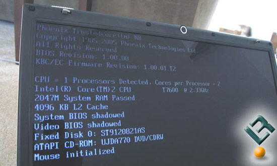
Correct BIOS Screen

Here is an image of the Clevo M570U posting and running the Core 2 Duo processor T7600 just fine with BIOS version 1.00.00 and upgraded to 1.00.02 with no issues at all. We also used Core 2 Duo on the ASUS Z97JS with pre-production BIOS V.080012 and the ASUS S96J with BIOS v0901. On the four notebooks we ran Merom on we had 100% success, but as you can tell it's hit or miss on the BIOS versions, so some research will need to be done before ALL updated and Core 2 Duo BIOS revisions are online. So to sum everything up if you've got a 945GM or 945PM Express chipset in your notebook, then the Core 2 Duo should be a drop in replacement for your Core Duo processor. If you don't have one of these chipsets then you'll need a whole new notebook to be able to run Core 2 duo processors!

Enough talk about BIOS revisions and let's take a look at Core 2 Duo!

Monday, April 6, 2009

Legit Reviews Visits Intel FAB 24-2 in Ireland

Taking The Tour of Intel's Leixlip Operations

Intel Ireland includes two facilities located in Leixlip and Shannon. Intel currently employees 5,125 people at their Ireland locations and has been in operation there since 1990. Legit Reviews recently had the oppurtunity to go on a private tour inside one of the FABs over in Leixlip and we would like share that expierence with our readers. Leixlip, located in County Kildare, is a tranquil community of approximately 15,000 people located 20 kilometers (12.5 miles) northwest of Dublin, Ireland's capital. The Leixlip FABs are Intel?s largest and most advanced manufacturing facilities outside of the United States.

Image Description

Leixlip consists of a number of manufacturing facilities, FAB?s 10/14 & FAB?s 24 & 24-2. FAB 10& FAB 14 are known as Ireland FAB operations (IFO). They operate on a 0.25, 0.18, 0.13, 0.090 and 0.065 micron production process. Between these two FABS Intel can produce 65 individual, different products. The IFO covers approximately 130,000sq meters. It is also the only source of the P854 & P856 chips used in many routers etc. It should also be pointed out that Intel Ireland has an excellent environmental management track record. Its Environmental Management System is accredited to the ISO 14001 quality standard and as such is the first Intel plant to do so. If you look at the above picture of the plant you can tell that it is located in a rural area, so being environmentally friendly is important!

Image Description

FAB 24 is one of the leading FABS to run 300mm technology on a 90nm process. 300mm wafers allow for high output at lower cost. FAB 24 is 52,000sq meters, which includes a 15,000sq meter clean room. It was opened in June 2004 and originally produced the Pentium 4 line of chips. FAB 24-2 is Intel?s new baby. It was only opened this summer back in June of 2006. I say it?s Intel?s baby, because it produces chips on the 65nm level. This is currently the smallest manufacturing process used for CPU?s and its home to the new Core 2 Duo chips, aka ?Conroe?.

My adventure started early in the morning, I had to catch a local train out to Leixlip and then take a long walk to reach Intel. The first thing I noticed when I arrived was the security. Not long after I arrived I was greeted by our contact in the main reception and after a quick security check I was allowed to pass through a metal detector. I should mention that no cameras were allowed inside the FAB?s (I said security was tight), so the pictures you?ll see were taken for us by Intel.

Intel IHS Lapping and Removal For LGA775 CPU's

Giving Intel Core 2 Duo A New Appearance

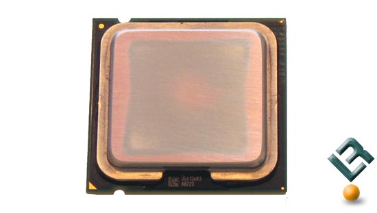
If you've maxed out your processor by overclocking and want to squeeze more out of it or are just looking to reduce core temperatures lapping the processor might be something worth looking into. All Intel LGA775 processors use the FC-LGA4 package, which means that the processor die is on top of the substrate on the opposite side from the LAND contacts. This package consists of a processor core mounted on a substrate land-carrier. An integrated Heat Spreader (IHS) is attached to the package substrate and core and serves as the mating surface for the processor component thermal solution such as a heat sink. Intel actually solders the IHS to the core of the processor, so the contact on the processor is usually not of concern. This brings us to the situation on hand. Many of the Allendale and Conroe processors that we have lapped have had heat spreaders that were not flat.

Intel LGA775 Conroe IHS Lapping

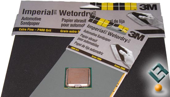
We went up to the local automotive supply store and picked up a number of different sandpaper packs ranging from 400 grit to 2500 grit. Using 2000 grit to 2500 grit sandpaper is far better than the factory finish, but for those that want to go crazy can invest in 1 micron diamond lapping compound to rub out all the sanding marks for a true mirror finish.

Intel LGA775 Conroe IHS Lapping

We took out Intel Core 2 Duo E6700 processor and started out lapping the IHS on a counter with 400 grit sand paper. After about 10 passes on the sandpaper it was obvious that the edges of the IHS were higher than the center, which means the hot core is not coming in direct contact with the base of our already lapped water cooling block.

Intel LGA775 Conroe IHS Lapping

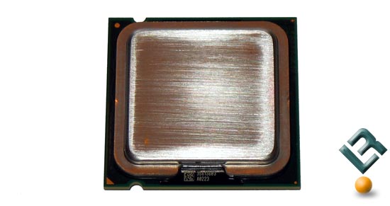
After a few minutes of 400 grit sanding we started to see copper that was previously hidden by the nickel plating that we have started to sand off. All Intel LGA775 processors feature copper integrated heat spreaders, so getting one of the flat will allow for great thermal transfer between the IHS and our copper water block. Once the block was flat and all the nickel was gone we moved on to finer sandpaper grits and called the surface of the IHS done after we used some 2500 grit paper on it.

Intel LGA775 Conroe IHS Lapping

The final result of lapping the processor was amazing. For less than twenty minutes worth of work we were able to take our Intel Core 2 Duo processor from having an uneven IHS to having a perfectly flat top hat. We took our lapped Intel Core 2 Duo E6700 Processor and ran it in the ABIT AW9D-MAX motherboard and found that the lapping reduced the idle temperatures by 2-3 degrees Celsius. Before the lapping it would idle 34-35C and after we were seeing 31-32C. Before we took load temperatures we thought we'd keep going and removed the IHS all together.

Monday, March 23, 2009

Intel Core 2 Extreme QX6700 Processor Review

Quad-Core Processors Arrive

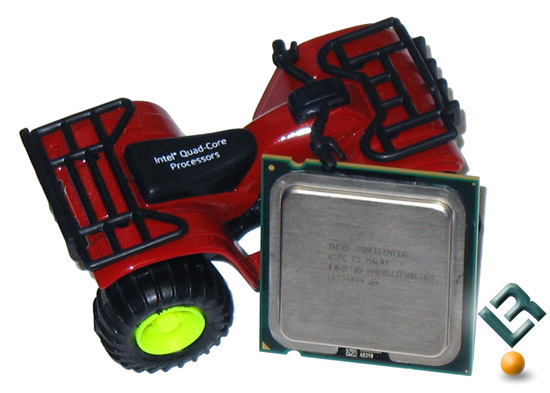
It's only been a few months since Intel slaughtered AMD?s reign on enthusiast desktop processors by releasing the Core 2 Duo family of processors, but it seems that Intel wants to see AMD squirm a little more and is launching the world?s first quad-core processor. The Intel Core 2 Extreme Processor QX6700 is undoubtedly aimed at the power user and just like any other Intel Extreme processor will set you back $999, like Extreme Editions have always been. Intel will keep the current Intel Extreme X6800 ?Conroe? processor around and the two will coexist for a while as some may want the extra clock speed versus the extra cores. As time goes on having more cores will lead to better performance across the board, so dual-core processors are already looking ?dated? as applications taking advantage of four or more cores are starting to appear on the horizon.

Image Description

Understanding how Intel came up with the Core 2 Quad processors is quite simple as Intel took two 'Conroe' cores from a Core 2 Duo processor and put them in a single 775-land multi-chip processor package (MCP) to provide much improved levels of perfromance of multi-media applications and multi-tasking usage models that take advantage of multiple cores. If we said that the majority of software applications on the market today takes full advantage of four or more cores it would be a lie, but the list of applications supporting four cores has been getting better as seen below.

Games Supporting 4+ Cores:

  • THQ Supreme Commander
  • Remedy Alan Wake
  • Valve Half-Life 2: Episode 2
  • Epic Unreal Engine 3
  • Ubisoft Splinter Cell: Double Agent

Multimedia Applications Supporting 4+ Cores:

  • Autodesk 3DSMAX 8 and 3DSMAX 9
  • Adobe After Effects 7/8
  • Adobe Premiere Pro 2/3.0
  • Adobe Encore DVD 2.+
  • Adobe Photoshop CS2
  • Maxon Cinema 4D v10 (TBD)
  • Pinnacle Studio dv 10
  • Quicktime Pro 7.1
  • XMPEG with DIVX 6.2
  • DVD Shrink 3.2
  • Pov Ray 3.7 Beta
  • Sony Vegas 7.0
  • Steinberg- Yamaha Cubase v4.5
  • TMPGEnc 2.524

Since many of the games and applications that support four or more cores are unreleased it is hard to look at the true potential of the Intel QX6700 processor. Legit Reviews has actually benchmarked the QX6700 with Intel last month and by using many of the above applications found that it was very impressive and showed a significant increase in performance. Since many of these applications have been covered this review will cover the standard benchmarks that LR has run for years to show how this flagship processor does on a wide variety of applications to better form an opinion on quad-core processors.

Intel Moves Closer to 45nm Penryn Processor Production

Intel Shows Off 45nm Progress Thanks To High-K Metal Gate Transistors

When things are going good companies like to brag and tout their stuff and that is exactly what Intel is doing tonight. With the embargo lifted on Intel's new 'High-k + Metal Gate Transistor Breakthrough' we can now talk about how Intel is now able to ramp up 45nm production for processors that will be coming out later this year on the mobile, desktop and server families.

Intel Metal Gate Transistors

Intel is pleased that the 'law' Gordon E. Moore came up with in 1965 is still holding true 42 years later now that we have entered in 2007. Back in 1965 Moore saw that the number of transistors on an integrated circuit doubles every 24 months. For those that have not seen the April 19th, 1965 Electronics Magazine copy here is what was said:

"The complexity for minimum component costs has increased at a rate of roughly a factor of two per year ... Certainly over the short term this rate can be expected to continue, if not to increase. Over the longer term, the rate of increase is a bit more uncertain, although there is no reason to believe it will not remain nearly constant for at least 10 years. That means by 1975, the number of components per integrated circuit for minimum cost will be 65,000. I believe that such a large circuit can be built on a single wafer."

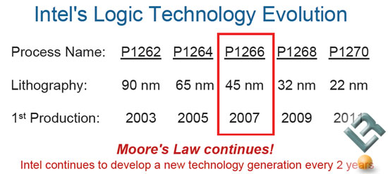
To keep up with Moore's Law Intel has had to keep shrinking the size of a processors core and has recently been able to produce processors on the 45nm process thanks to improvements in the way transistor gates have been made.

Intel Metal Gate Transistors

Compared to Intel's current 65nm process the 45nm process they moving over to is said to double the transistor density, while also improving leakage and performance levels. The performance and leakage improvements are due to the fact that Intel has now successfully developed a method to produce high-k + metal gate transistors.

Intel Metal Gate Transistors

Not much has changed over the years when it comes to transistors, but that is no longer true now that high-k + metal gate transistors have been shown to work in real life. Intel has had working high-k + metal gate transistors since 2003, but just recently has been able to implement the technology with the 45nm manufacturing process that will ramp up later this year. The 'new' parts of this transistor are the gate dielectric now consists of a 'high-k' material and the gate electrode itself is now made of metal. By converting SiO2 gate dielectric to high-k it allows thickening the dielectric layer while also increasing the gate field effect resulting in increased “on”current, decreased “off”current and significantly decreased gate leakage.

Intel Metal Gate Transistors

By moving from polysilicon gate transistors to metal gate transistors Intel has been able to improve the drive current by greater than 20% and has significantly reduced leakage. After hearing of the news of the new transistor, Intel co-founder Gordon Moore made the following statement:

'The implementation of high-k and metal gate materials marks the biggest change in transistor technology since the introduction of polysilicon gate MOS transistors in the late 1960s'

Now that we have covered the technical aspect of the high-k + metal gate transistors that make 45nm processor a reality we can see what this means for consumers in the second half of this year.

Friday, March 20, 2009

Intel Penryn and Nehalem 45nm Processor Update

Intel Briefs The Press on Penryn and Nehalem Processors

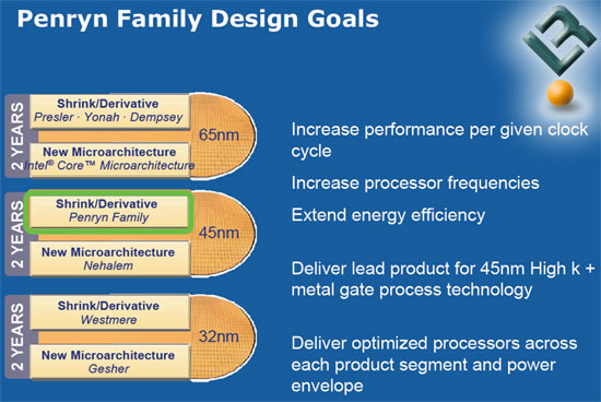
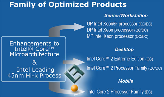
Marking the next step in Intel’s “tick-tock” product strategy and cadence to deliver a new process technology with an enhanced microarchitecture or entirely new microarchitecture every year, Intel Corporation will begin producing its next-generation Penryn family of processors in the second half of this year. These new processors benefit from enhancements to the Intel Core™ microarchitecture and also Intel’s industry-leading 45nm Hi-k process technology with its hafnium-based high-k + metal gate transistor design, which results in higher performance and more energy-efficient processors.

Intel Penryn and Nehalem CPU Microarchitecture Technology

Intel has more than 15 45nm Hi-k product designs in various stages of development, and will have two 45nm manufacturing fabs in production by the end of the year, with a total of four in production by the second half of 2008 that will deliver tens of millions of these processors. Below are many of the details of the Penryn processor family and a glimpse into some of the key features of Intel’s future generation of processors, codenamed Nehalem.

Intel Penryn and Nehalem CPU Microarchitecture Technology

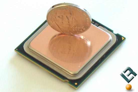
The 45nm next-generation Intel Core 2 quad-core processors will have 820 million transistors. Due to Intel's high-k metal transistor invention, think of 820 million more power efficient light bulbs going on and off at light-speeds. The dual-core version has a die size of 107mm2, which is 25 percent smaller than Intel’s current 65nm products -- and quarter of the size of the average postage stamp -- and operate at the same or lower power than Intel’s current dual core processors.

Intel Penryn and Nehalem CPU Microarchitecture Technology

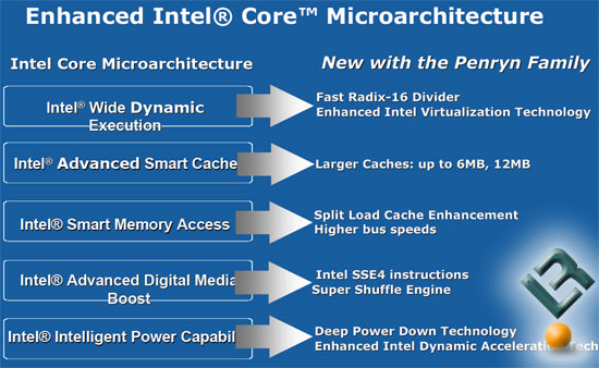
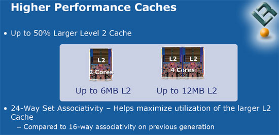
Penryn processors include up to a 50 percent larger L2 cache with a higher degree of associativity to further improve the hit rate and maximize its utilization. Dual-core Penryn processors will feature up to a 6MB L2 cache and quad-core processors up to a 12MB L2 cache. Cache is a memory reservoir where frequently accessed data can be stored for more rapid access. Larger and faster cache sizes speed a computer’s performance and response time.

Intel Penryn and Nehalem CPU Microarchitecture Technology

Six Penryn family processors, including dual and quad-core desktop processors and a dual core mobile processor are all under the Intel Core processor brand name as well as new dual and quad-core server processors under the Intel Xeon processor brand name. A processor for higher-end server multiprocessing systems is also under development. As previously noted, Intel already has a total of 15 45nm products scheduled.

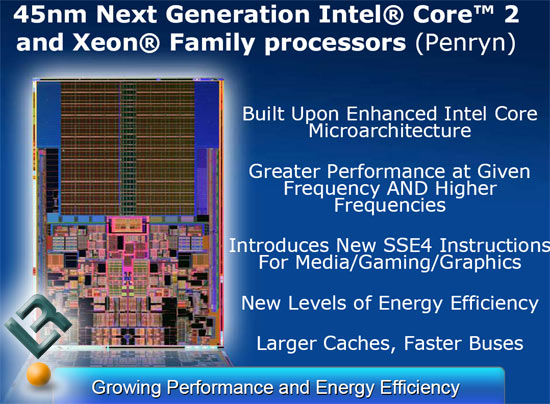
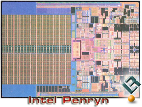
Intel Penryn CPU Die

All of these features and cache are jam packed into the single piece of silicon that makes up the processor. Above is the die photo oh Penryn for those that would like to see what it looks like. Intel has a number of these processors already up and running and just today showed the media a technology demo that included games on a Windows XP Professional platform using Penryn.

Intel Penryn 3.33GHz Processor Benchmarks

Intel Releases Wolfdale & Yorkfield Benchmark Numbers

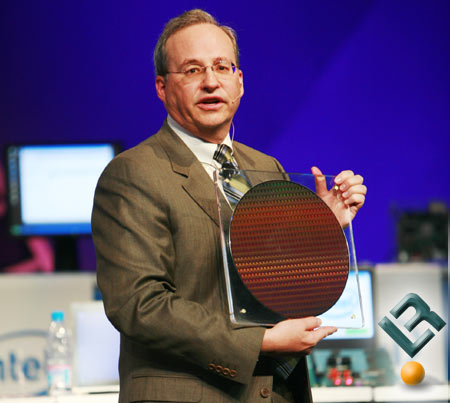
Justin Rattner with Penryn Wafer

With the Beijing 2007 Intel Developer Forum in full swing the amount of information that is coming out on Penryn is nothing short of amazing. Intel has even gone as far as showing performance numbers and has had systems up and running with these 45nm processors this week in Beijing, China. Legit Reviews has recently covered the upcoming Penryn and Nehalem 45nm processors, so be sure to read up on our previous coverage to better understand the changes that are coming.

Justin Rattner with Penryn Wafer

To quickly sum up Penryn for the desktop market, there will be two versions. One will be a quad-core varient with 12MB L2 cache and the other will be a dual-core part with just 6MB L2 cache, since it is missing a core.

Justin Rattner with Penryn Wafer

Current Core 2 Duo and Core 2 Quad processors have 16-way associativity, but on Penryn this number has been increased to 24-way associativity, which improves the access paths to the larger L2 cache. Other than the performance improvements that are taking place in the cache the Penryn processors have a new SSE4 instruction that can be used on various media, gaming, and graphic applications. Now that we have a quick background on the processors lets skip on to the performance numbers!

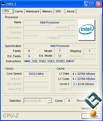
Intel Yorkfield CPU-Z Screenshot

With CPU-Z 1.38 loaded on the Intel test system we can see what a quad-core Yorkfield 45nm processor shows up as in the test system!